


BUILDING THE FUTURE...RIGHT NOW!!
PCB@SAelectronics.org
847-380-3017
We Supply B2B & Personal

25 YEARS OF EXPERIENCE
-
BLIND AND BURIED VIAS
-
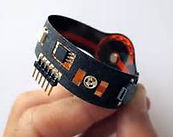
RIGID-FLEX & FLEX PCB
-
IPC Class 3 QUALITY
Why use HDI's?
-
Micro via formation technology using lasers has become the dominant method for drilling micro vias that are also called blind via-holes (BVHs) in printed circuit boards (PCBs).
-
We use a plate shut process which gives our clients more reliability for micro via process’s than filled with non-conductive ink and then plating over.
-
This technology allows future components, that are becoming smaller, to be used on a wider scale.
-
Electrical performance: The smaller parts used on HDI boards, have shorter internal wire lengths, reduced rise times, and lower power requirements when compared to their larger, alternative packages.
-
Creating a gateway to Miniaturization of PCB design with ‘Via in Pad’ technology.
-
Improved reliability by stepping up technology rather than compromising existing design rules.
-
Giving a wider array of design choices when it comes to BGA layout with the smallest pitch.
-
Opportunities for better thermal enhancement.
-
Increasing interconnection density by reducing plated thru holes, pad size and conductor size reduction.
-
Provides to have via hole connected directly on the surface mount pad or BGA pad.
HDI
HIGH DENSITY INTERCONNECTS
-
HDI is the abbreviation for High Density Interconnector. HDI PCB is defined as a PCB with a higher wiring density per unit area than conventional PCB. They have finer lines and spaces, smaller vias and capture pads and higher connection pad density than employed in conventional PCB technology. HDI PCB is used to reduce size and weight, as well as to enhance electrical performance of the device. HDI PCB is made through Microvia and buried vias and sequential lamination with insulation materials and conductor wiring for higher density of routing. HDI PCB is the best alternative to high layer-countand expensive standard laminate or sequentially laminated boards.
-
HDI (high density interconnection) circuit boards and Micro via Technology are very closely linked. Micro vias are holes drilled using a laser drilling process. The purpose for these holes is to create electrical connection in between the layers on a multilayer circuit board design.
-
Via in Pad micro vias play a key role in the process of shrinking down the PCB size. These holes are not to be used for inserting a component lead or any other reinforcing material. However, the ability to either place on or off the pads gives the designers greater flexibility to selectively create routing room in denser parts of the substrate.


Continuation of this article is in
The PCB Magazine (2015). http://iconnect007.uberflip.com/i/490885-pcb-apr2015
There were a lot of different names for the PCB with such structures. For example, it was called SBU (Sequence Build up the Process) in European and American industry as the program production is in the constructive mode of sequence. It was called MVP (Microvia Process) in Japanese industry because the hole of such products is much smaller than the previous one. It was also called BUM (Build up Multilayer Board) because the traditional multilayer is known as MLB (Multilayer Board).In order to avoid confusion, IPC Printed Circuit Association proposed to call it HDI (High Density Interconnection Technology) as the common name, but it can not reflect the characteristics of the circuit board. So the majority in the PCB industry define such products as HDI PCB.